

Boosting the performance of solar cells, transistors, LEDs, and batteries hinges on the discovery and development of better electronic materials with novel compositions. Scientists are increasingly turning to AI tools to sift through hundreds of millions of chemical formulations, identifying promising candidates for advanced functional materials. Simultaneously, engineers are creating high-throughput printing machines capable of producing hundreds of material samples based on these AI-identified compositions.
However, a significant bottleneck has persisted in confirming the performance of these printed materials. The characterization process, a crucial last step, has lagged behind, hindering the rapid screening of advanced materials.
MIT engineers have now addressed this challenge with a novel computer vision technique that dramatically speeds up the characterization of newly synthesized electronic materials. This technique automatically analyzes images of printed semiconducting samples, rapidly estimating two critical electronic properties: band gap (a measure of electron activation energy) and stability (a measure of longevity).
Astonishingly, this new technique characterizes electronic materials 85 times faster than the current standard approach. The researchers plan to deploy this technique to accelerate the search for promising solar cell materials and integrate it into a fully automated materials screening system.
“Ultimately, we envision fitting this technique into an autonomous lab of the future,” says MIT graduate student Eunice Aissi. “The whole system would allow us to give a computer a materials problem, have it predict potential compounds, and then run 24-7 making and characterizing those predicted materials until it arrives at the desired solution.”
The application space for these techniques ranges from improving solar energy to transparent electronics and transistors,
adds MIT graduate student Alexander (Aleks) Siemenn.
It really spans the full gamut of where semiconductor materials can benefit society.
Aissi and Siemenn, along with their MIT colleagues, detail their innovative technique in a study published in Nature Communications.
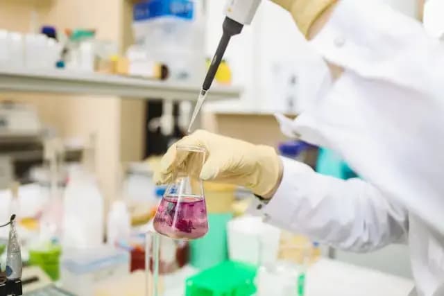
Traditionally, characterizing a newly synthesized electronic material involves a “domain expert” meticulously examining each sample using a UV-Vis tool. This manual process, while precise, is time-consuming, with an expert typically characterizing about 20 material samples per hour. This pace pales in comparison to modern printing tools that can deposit 10,000 different material combinations in the same timeframe.
“The manual characterization process is very slow,” says Professor Tonio Buonassisi of MIT. “They give you a high amount of confidence in the measurement, but they’re not matched to the speed at which you can put matter down on a substrate nowadays.”
Recognizing the need to accelerate the characterization process, Buonassisi and his team turned to computer vision, a field leveraging computer algorithms to rapidly analyze optical features in images.
“There’s power in optical characterization methods,” Buonassisi notes. “You can obtain information very quickly. There is richness in images, over many pixels and wavelengths, that a human just can’t process but a computer machine-learning program can.”
The team recognized that specific electronic properties, particularly band gap and stability, could be estimated solely from visual information if captured with sufficient detail and interpreted accurately.
Driven by this insight, the researchers developed two novel computer vision algorithms to automatically interpret images of electronic materials: one for estimating the band gap and the other for determining stability.
The first algorithm processes visual data from highly detailed hyperspectral images. “Instead of a standard camera image with three channels — red, green, and blue (RBG) — the hyperspectral image has 300 channels,” Siemenn explains. “The algorithm takes that data, transforms it, and computes a band gap. We run that process extremely fast.”
The second algorithm analyzes standard RGB images, assessing a material’s stability by tracking visual changes in its color over time.
“We found that color change can be a good proxy for degradation rate in the material system we are studying,” Aissi says.
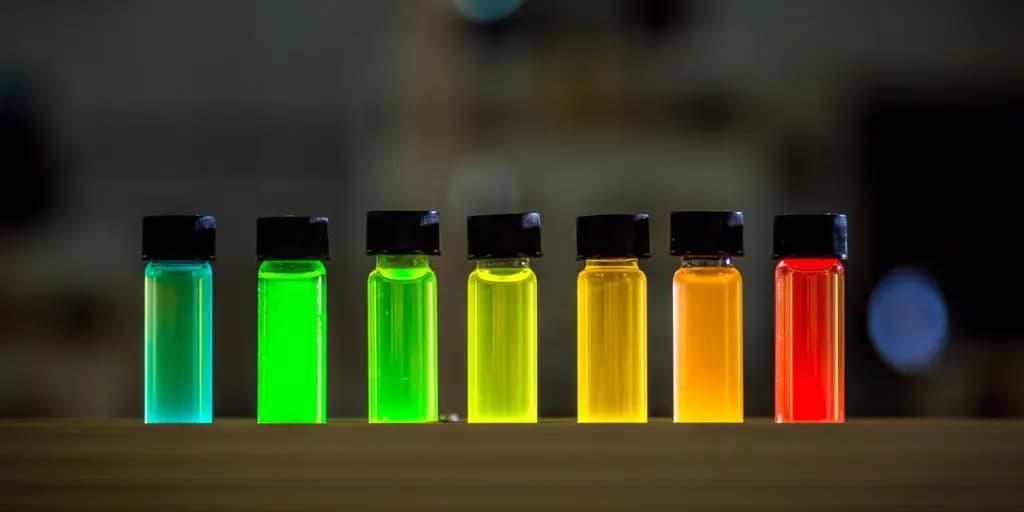
To validate their algorithms, the team used them to characterize the band gap and stability of approximately 70 printed semiconducting samples, each with a slightly different composition of perovskites—a material class considered a promising candidate for solar cells despite its known rapid degradation.
The team printed these diverse perovskite compositions onto a single slide using a robotic printer. They then scanned the slide with a hyperspectral camera and applied their band gap algorithm to the automatically segmented sample images. The entire band gap extraction process took a mere six minutes, a task that would typically require several days for a domain expert to complete manually.
“It would normally take a domain expert several days to manually characterize the same number of samples,” Siemenn points out.
To assess stability, the team subjected the slide to varying environmental conditions (humidity, temperature, and light exposure) within a chamber, capturing images of the samples every 30 seconds for two hours using a standard RGB camera. By analyzing these images with their second algorithm, they estimated the color change, or degradation, of each sample over time, generating a “stability index” for each.
Impressively, the team‘s band gap and stability results were 98.5 percent and 96.9 percent as accurate as the expert’s benchmark estimates, respectively, while being 85 times faster.
“We were constantly shocked by how these algorithms were able to not just increase the speed of characterization, but also to get accurate results,” Siemenn remarks. “We do envision this slotting into the current automated materials pipeline we’re developing in the lab, so we can run it in a fully automated fashion, using machine learning to guide where we want to discover these new materials, printing them, and then actually characterizing them, all with very fast processing.”
Image courtesy: Bryce Vickmark.
The link to the original cover story can be accessed here.
The original research paper (open access) can be accessed here.


Responses (0 )